A CMOS transistor and the bipolar junction transistors which are two separate technologies of semiconductors and are integrated into a single integrated circuit device using an evolved and enhanced semiconductor technology known as BiCMOS.

We use many electric appliances in our daily life. Each of which consists of motors, wires, semiconductors, etc. Using the fabrication process of these semiconductor devices, integrated circuits are manufactured. Each and every component of the electronic and electrical devices is interlinked with each other using these integrated circuits. A wafer is used to create the electronic circuits. The wafer is made up of some semiconductor compounds which involve several steps of chemical and photo lithography processes, some other pure semiconductor materials such as silicon.
This process of manufacturing of semiconductors is now spread all over the world. But its roots have started in early 1960’s from Texas. Due to its need it is being deployed and implemented.
BiCMOS Technology
In 1990’s this technology is one of the highly developed and the major semiconductor technologies. It is combined with two major separate technologies in a single modern integrated circuit such as CMOS transistor and the bipolar junction transistor.
To understand and implement this technology to the best, it is needed for you to have the better understanding and the knowledge of the Bipolar and CMOS technologies.
This is the first digital or analog receiver Integrated circuit. This BiCMOS integrated receiver is of very high sensitivity.

CMOS Technology
The reason and the need behind its invention is the need of electronic calculators. They are started as sources for calculators. It is a complementary technology of CSG (Commodore Semiconductor Group) or MOS technology which is known as CMOS technology.
The main motto of this CMOS technology is to develop the digital logic circuits which are one of the integrated circuits. They are implemented along with the microprocessors and the microcontrollers. The main advantage and feature of this CMOS technology is that it provides and enhances the benefits of dissipation of less power. With high packing density, it also allows the low noise margin.

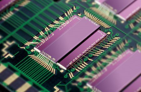
This is how CMOS technology is used for manufacturing of switch devices that are controlled digitally as shown in the figure.
Advantages of BiCMOS technology
o Usage of CMOS circuit of high impedance as input improves and facilitates the design of Analog amplifier. Bipolar transistors are used for rest of them.
o A good economical consideration in electrical parameters with less variability is possible by the variations of BiCMOS process.
o As per the requirement, BiCMOS devices can provide the high load current sourcing and sinking.
o When compared to bipolar technology, it allows low power dissipation.
Drawbacks of BiCMOS technology
o This process is quite complex as both the bipolar and CMOS technologies are included in the fabrication process of this technology.
o As the complexity is high in the manufacturing process, the cost is also more.
o Here there is a chance of less lithography as it consists of more and more devices.


